


Ceramic vs Sapphire Components for Optical and Semiconductor Applications: A Material Selection Guide
- Muhammad Kazim
- Jul 14
- 7 min read


Choosing between technical ceramic and sapphire components in semiconductor and optical systems is rarely straightforward. Both materials offer exceptional hardness, chemical inertness, and thermal stability — but their performance profiles diverge sharply under the specific process conditions that define real-world semiconductor fabrication and precision optical assemblies. If you're sourcing semiconductor ceramic components for plasma etch chambers, wafer handling equipment, UV optical windows, or high-purity chemical processing lines, this comparison will give you the material-level data needed to make the right call.
Sourcing custom semiconductor components with tight tolerances? Submit your technical drawings to the MAC engineering desk to Request an RFQ in 24 Hours
What We Mean by "Technical Ceramics" in This Context
Technical ceramics — also called advanced ceramics or engineering ceramics — are inorganic, non-metallic materials engineered for specific mechanical, thermal, electrical, or chemical properties. In semiconductor and optical applications, the most commonly specified grades are:
Aluminum oxide (alumina, Al₂O₃) — 96% to 99.8% purity grades
Aluminum nitride (AlN) — high thermal conductivity variant
Silicon carbide (SiC) — either sintered or reaction-bonded
Zirconia (ZrO₂) — typically yttria-stabilized
Silicon nitride (Si₃N₄) — for high-stress structural applications
These are processed via dry pressing, isostatic pressing, or injection molding, then sintered at high temperature to achieve near-theoretical density.
Sapphire, by contrast, is single-crystal aluminum oxide (Al₂O₃) — chemically the same compound as alumina, but grown as a continuous crystal lattice via the Czochralski or Kyropoulos process. The single-crystal structure eliminates grain boundaries, which fundamentally changes how the material behaves in optical and surface-sensitive environments.
Key Material Properties: Side-by-Side Comparison
The table below compares the most specification-relevant properties for procurement engineers evaluating both materials. Values reflect typical published ranges; confirm against specific lot certifications for critical applications.
Property | Alumina (99.8%) | Sapphire (Single Crystal) | AlN | SiC (Sintered) |
Crystal Structure | Polycrystalline | Single crystal | Polycrystalline | Polycrystalline |
Hardness (Vickers) | ~1,800 HV | ~1,800–2,000 HV | ~1,200 HV | ~2,500 HV |
Flexural Strength | ~380 MPa | ~400–690 MPa (orientation-dependent) | ~320 MPa | ~400–500 MPa |
Max Operating Temp (non-oxidizing) | 1,700°C | 1,800°C [VERIFY] | 1,000°C (in air) | 1,650°C |
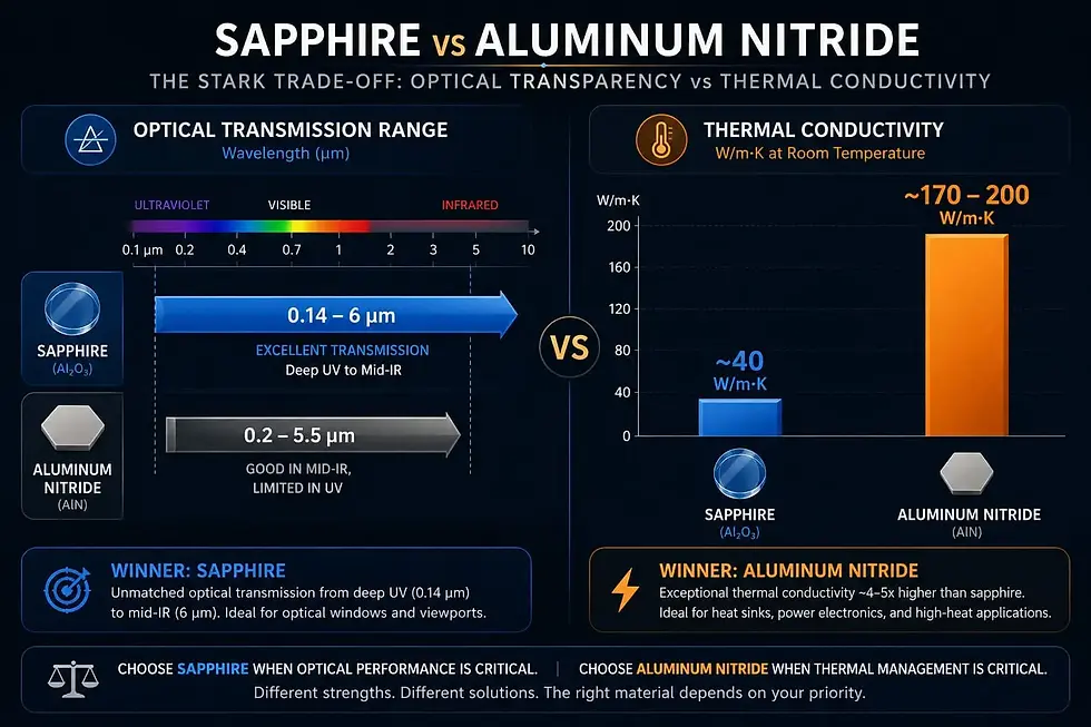
Thermal Conductivity | ~35 W/m·K | ~40 W/m·K | ~170–200 W/m·K | ~120 W/m·K |
Thermal Expansion (CTE) | ~8.1 ppm/°C | ~5.0–6.6 ppm/°C (c-axis) | ~4.5 ppm/°C | ~4.0 ppm/°C |
Optical Transmission Range | None (opaque) | 0.14–6 µm (UV to mid-IR) | None (opaque) | None (opaque) |
Surface Roughness (achievable Ra) | <0.1 µm | <0.5 nm (polished) | <0.2 µm | <0.05 µm |
Typical Purity (Al₂O₃ content) | 99.5–99.8% | 99.999%+ | N/A | N/A |
Relative Cost | Low–Medium | High | Medium–High | Medium–High |
All values are typical; actual specifications depend on grade, processing method, and geometry. Dimensional tolerances achievable to ±0.005" on standard features; tighter tolerances to ±0.001" on request. [VERIFY tolerances with MAC engineering team for application-specific parts.]
Where Each Material Dominates
Sapphire: When Optical Transparency and Surface Perfection Are Non-Negotiable
Sapphire's defining advantage is its broadband optical transmission — from deep UV (~150 nm) through the visible spectrum and into the mid-infrared (~6 µm). No polycrystalline ceramic can match this. In semiconductor fabs, this matters in:

Optical windows for plasma process chambers — sapphire withstands fluorine-based plasma chemistries (CF₄, SF₆) and provides a clean optical path for endpoint detection sensors
UV lithography optics and beam delivery — where transmission at 193 nm (ArF excimer laser wavelength) is critical
EUV and deep-UV inspection windows — high transmission, low absorption loss
Laser diode facets and substrates — particularly in GaN-on-sapphire epitaxial processes
The single-crystal structure also means sapphire has no grain boundaries that can preferentially etch, delaminate, or contribute contamination. This is particularly relevant in wet chemical processes and ultrapure DI water environments where polycrystalline alumina can release particles at grain boundaries over time.
Surface finish capability for sapphire is extraordinary — optical-grade polishing achieves Ra values below 0.5 nm, enabling use as precision reference flats, etalons, and optical substrates.
Technical Ceramics: When Structural Performance, Thermal Management, and Cost Drive the Decision
Polycrystalline ceramics — particularly alumina, AlN, and SiC — cover the much larger design space where optical transparency is not required. They offer:
Alumina (Al₂O₃, 99.8%): The workhorse of semiconductor ceramic components. Cost-effective, chemically resistant to most acids and bases, compatible with high-vacuum environments, and available in virtually any geometry. For advanced process nodes, high-purity alumina ceramics for semiconductor equipment provide the necessary baseline to prevent trace contamination.
Common applications include:
Wafer handling paddles and susceptors
Etch chamber liners and focus rings
High-voltage insulators in ion implant systems
Carrier components in diffusion furnaces
Aluminum Nitride (AlN): When thermal management is the design constraint. With thermal conductivity of 170–200 W/m·K [VERIFY SOURCE], AlN is used in electrostatic chucks (ESCs), heater substrates, and wafer pedestals where heat uniformity across the wafer directly impacts process yield. CTE matching to silicon (~3.5 ppm/°C for Si vs. ~4.5 ppm/°C for AlN) reduces thermally induced stress at elevated chuck temperatures.

Silicon Carbide (SiC): Preferred for extreme wear, high stiffness-to-weight ratio applications, and environments where alumina's chemical resistance is insufficient. SiC components appear in chemical mechanical planarization (CMP) retaining rings, high-temperature structural parts, and abrasive slurry handling systems.
Critical Selection Criteria for Procurement and Design Engineers
1. Optical Function Required?
If any optical path, sensor window, or light transmission is involved — even incidentally — sapphire is likely the required material. No polycrystalline ceramic alternative exists for true UV-VIS-IR transmission. If optical function is absent, technical ceramics will almost always deliver a better cost-to-performance ratio.
2. Chemical Compatibility Matrix
Both sapphire and high-purity alumina resist most mineral acids. However:
Sapphire shows superior resistance to hydrofluoric acid (HF) environments compared to polycrystalline alumina at elevated temperatures — grain boundary effects in polycrystaline materials accelerate attack
AlN is attacked by water and acid; not suitable for wet chemistry exposure without protective coatings
SiC offers superior resistance to oxidizing acids but can be attacked by molten alkalis
Always map your process chemistry against material-specific chemical resistance data, not just generic "ceramic" ratings.
3. Dimensional Tolerances and Geometry
Sapphire is machined from grown boules — maximum achievable part size is constrained by crystal growth limits. Large-diameter or complex 3D geometries are significantly more expensive in sapphire than in ceramic, where near-net-shape forming via pressing or injection molding enables cost-effective complex geometries.
For precision bore diameters, flatness specifications, and parallelism on optical flats, both materials can achieve tight tolerances when ground by capable manufacturers — but the process and tooling cost differ substantially.
Note: Our engineering team regularly works with custom CAD drawings to optimize complex geometric features and significantly lower machining costs. If you are designing for sub-mil precision, Consult with a MAC Engineer to optimize your custom components
4. Thermal Cycling and CTE Matching
In bonded assemblies (ceramic-to-metal or ceramic-to-silicon), CTE mismatch is a primary failure mode under thermal cycling. Sapphire's CTE varies by crystallographic orientation (c-axis vs. a-axis), which can complicate bonded joint design. For CTE-matched applications to silicon, AlN is often the preferred technical ceramic.
5. Volume and Lead Time
Sapphire components, especially optically polished or large-diameter parts, carry long lead times — crystal growth is slow, and machining is abrasive and labor-intensive. For high-volume procurement or applications tolerant of polycrystalline microstructure, technical ceramics offer faster lead time and more consistent pricing at volume.
Why Material Source and Manufacturing Capability Matter as Much as Material Choice
Even the correct material specification delivers subpar results if the component manufacturer lacks the machining precision, quality systems, and material traceability to hold tolerances in production. In semiconductor and optical applications, this means:
ISO 9001-certified quality management — mandatory for fab-qualified supplier programs
Dimensional inspection to ±0.001" or better on critical features [VERIFY achievable tolerance range]
Material certification and lot traceability — particularly relevant for alumina purity grades and sapphire crystal orientation
Surface finish verification — profilometry data, not just stated Ra values
Microns Advanced Ceramics (Hayward, CA) manufactures precision technical ceramic components for semiconductor OEMs, with machining capability across alumina, AlN, SiC, and zirconia. Their engineering team works from customer drawings to recommend material grade, geometry, and tolerance stack-up — which is particularly useful when evaluating a switch from an incumbent sapphire component to a technical ceramic alternative for cost reduction without performance compromise.
Closing: Ceramic or Sapphire — Make the Call Based on Function, Not Familiarity
The default instinct to specify sapphire for any "precision" semiconductor application is understandable but often unnecessary. Sapphire earns its place when optical transmission, single-crystal surface integrity, or extreme purity is genuinely required by the process. In the majority of structural, chemical-resistant, and thermally demanding semiconductor component applications, engineered technical ceramics deliver equivalent or superior performance at lower cost and shorter lead time.
The right answer is always function-first: map the actual process requirements — temperature, chemistry, optical path, mechanical load, surface finish, and tolerance — against the material property table, and let that drive the specification.
Partner with a US-Based Precision Ceramics Leader
Selecting the ideal advanced material and navigating tight tolerance requirements shouldn't introduce bottlenecks to your production schedule. Microns Advanced Ceramics manufactures custom, high-purity components right here in Hayward, CA, pairing ISO 9001 quality standards with rigorous material traceability and design-for-manufacturability (DFM) support. Whether you are replacing an costly sapphire component or looking to scale a custom technical ceramic run, our engineering team works directly with your procurement goals.
Looking for specialized solutions? Speak directly with our Hayward Engineering Desk or explore our dedicated line of Semiconductor Ceramic Components.
Ready to evaluate ceramic component options for your semiconductor or optical application?
Submit an RFQ or contact the Microns Advanced Ceramics engineering team to discuss material selection, tolerances, and prototype lead times for your specific geometry. If your project requires custom precision ceramic components in Hayward, CA, MAC works directly with procurement teams and design engineers to provide material recommendations, DFM feedback, and certified production components.
Key Takeaways
Sapphire is single-crystal Al₂O₃ — its optical transparency (UV to mid-IR) and grain-boundary-free surface make it irreplaceable for optical windows, UV substrates, and plasma-chamber viewports; polycrystalline ceramics cannot substitute in these roles.
Technical ceramics (alumina, AlN, SiC) dominate non-optical semiconductor applications — structural components, wafer handling, insulators, and process chamber liners — at lower cost and faster lead time than sapphire.
AlN is the preferred ceramic for thermal management in wafer chucks and heater substrates due to its high thermal conductivity (~170–200 W/m·K) and close CTE match to silicon.
Chemical compatibility varies by specific grade and process chemistry — do not rely on "ceramic" as a blanket specification; validate against your exact etchant, solvent, or cleaning chemistry.
Manufacturer capability is as critical as material selection — ISO 9001 certification, dimensional inspection data, and material traceability documentation should be part of any supplier qualification for semiconductor ceramic components.
Technical values in this article are representative of published material property ranges. Confirm all specifications against material certifications and manufacturer data sheets before use in production applications. Items marked [VERIFY] should be confirmed with the MAC engineering team prior to publication.


Comments