


Electrostatic Chuck Ceramic: Alumina vs AlN Guide

Written by: Gulzar Hussain · Reviewed by: Mark Ma, Lead Materials Engineer ·
Who this is for: equipment and process engineers specifying or replacing ESC ceramics for etch, CVD, PVD, or implant tools.
An electrostatic chuck ceramic is the dielectric layer that clamps a wafer by electrostatic force inside a vacuum process chamber. High-purity alumina is the standard for Coulombic chucks. Doped alumina or aluminum nitride, tuned to a partially conductive resistivity at operating temperature, is used for Johnsen-Rahbek (J-R) chucks.
This guide explains how the ceramic's resistivity decides which chuck type you get, and when AlN is worth its cost over alumina. It also covers the design features and failure modes you need to know before you send an RFQ.
Key takeaways
Volume resistivity at operating temperature is the most important ESC ceramic specification.
Coulombic chucks need a highly insulating dielectric. J-R chucks need a controlled, partially conductive one.
AlN wins on thermal conductivity and CTE match to silicon. Alumina wins on cost, availability, and machinability.
Most ESC failures trace back to resistivity drift, gas-hole arcing, or mesa wear. The material is rarely the cause on its own.
Refurbishment can extend chuck life, but only if dielectric thickness over the electrode is measured and controlled.

What is an electrostatic chuck and where does the ceramic sit?
An electrostatic chuck (ESC) holds the wafer flat and controls its temperature during plasma and deposition steps. Mechanical clamps touch the wafer edge, and vacuum chucks can't work in a vacuum chamber. An ESC clamps the whole back surface with no contact on the front side.
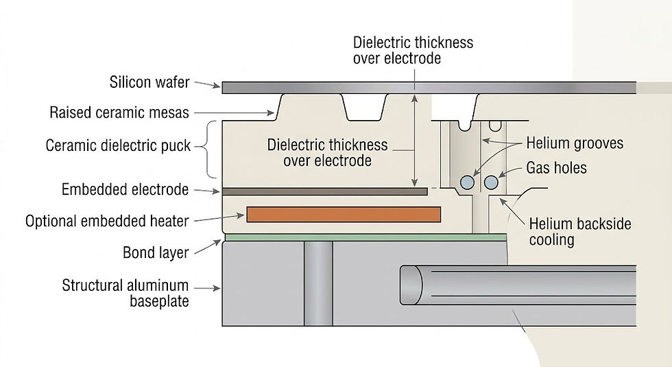
A typical ESC stack, from top to bottom:
Wafer, resting on raised mesas.
Ceramic dielectric puck (the electrostatic chuck ceramic), carrying mesas, helium grooves, gas holes, and lift pin holes.
Embedded electrode: monopolar (wafer grounded through plasma) or bipolar (works without plasma).
Optional embedded heater, for CVD and other high-temperature processes.
Bond layer joining the puck to the base.
Cooled aluminum baseplate with coolant channels.
The ceramic does four jobs at once. It is a controlled dielectric, a thermal path to the baseplate, a flat reference surface, and a plasma-resistant barrier that must not shed particles or metals onto the wafer.
Coulombic vs Johnsen-Rahbek: how resistivity decides the chuck type
The ceramic's volume resistivity decides where electric charge sits during clamping. That decides which clamping mechanism you get.
Coulombic chucks use a highly insulating dielectric. Charge stays at the electrode, and the clamping force acts across the full dielectric thickness. Sintered-AlN patent literature puts clean release and low leakage at a volume resistivity of about 10^15 Ω·cm or higher. That is why high-purity alumina is the conventional Coulombic material.
Johnsen-Rahbek chucks use a partially conductive dielectric. Charge migrates to the wafer contact surface, so the effective gap is tiny and the force per volt is much higher. The drawbacks are higher leakage current and residual surface charge that can make the wafer hard to release.
For J-R operation, the published window is roughly 10^8 to 10^13 Ω·cm at operating temperature, with 10^9 to 10^11 Ω·cm preferred. A dry etch chuck must hit that near room temperature. A PVD or CVD chuck must hit it at roughly 250 to 700 °C.
Factor | Coulombic ESC | Johnsen-Rahbek ESC |
Dielectric resistivity | High (about 10^13 to 10^15+ Ω·cm) | Controlled (about 10^9 to 10^11 Ω·cm at temperature) |
Typical ceramic | High-purity alumina, high-resistivity AlN | Doped alumina, doped AlN |
Clamping force per volt | Lower | Higher |
Operating voltage | Higher | Lower |
Leakage current | Very low | Higher, needs a larger power supply |
Dechuck behavior | Fast, clean release | Residual charge can cause sticking |
Temperature sensitivity | Lower | High, resistivity falls as temperature rises |
Engineer's note: always specify resistivity at operating temperature, not only at room temperature. A ceramic in the J-R window at 25 °C can drop into excessive leakage at 400 °C. A room-temperature value alone is not enough for a heated chuck.
How dopants tune the ceramic
Pure alumina is too insulating for J-R operation. Adding 1 to 3 wt% titania lowers its resistivity to about 10^11 to 10^13 Ω·cm, which is why doped alumina is used for J-R chucks. The trade-off is that its resistivity keeps falling as temperature rises, and leakage can outgrow the chuck power supply.
Undoped AlN goes the other way. At room temperature it is generally above 10^13 Ω·cm, too high for J-R use, so manufacturers lower it with small additions of metals or carbon.
Dopant choice also affects heat transfer. A 2025 study of rare-earth-doped AlN found Y2O3-doped samples could exceed 250 W/m·K. Other dopants stayed below 200 W/m·K because they formed heat-resistant phases at grain boundaries.
Alumina vs aluminum nitride for ESC ceramics
Both materials are proven in production tools. The right choice depends on heat load, operating temperature, chuck type, and budget.

Property (typical, grade-dependent) | High-purity alumina (99.5 to 99.9%) | Aluminum nitride (AlN) |
Density (g/cm³) | 3.9 | 3.3 |
Thermal conductivity (W/m·K) | 25 to 35 | 150 to 200+ |
CTE, 20 to 400 °C (10^-6/K) | 7 to 8 | 4.5 to 5 (silicon about 2.6) |
Dielectric constant, 1 MHz | 9.5 to 10 | 8.5 to 9 |
Volume resistivity, undoped, RT (Ω·cm) | above 10^14 | above 10^13 |
Flexural strength | 300 to 400 MPa (43 to 58 ksi) | 300 to 350 MPa (43 to 51 ksi) |
Fracture toughness (MPa·m½) | 3.5 to 4.5 | 2.5 to 3.5 |
Relative cost | Lower | Higher |
Typical ESC role | Coulombic; doped for J-R | Heated chucks; doped for J-R |
Values are typical published ranges. Confirm against the specific grade datasheet.
Choose alumina when:
The process runs near room temperature with moderate heat flux.
You need a Coulombic chuck with fast, clean dechuck.
Cost and lead time drive the decision, or the part is a sprayed-dielectric refurbishment.
Choose AlN when:
Heat flux is high and wafer temperature uniformity limits yield.
The chuck has an embedded heater, as in CVD. AlN chucks with heaters are commercially rated to about 500 °C.
Thermal cycling makes CTE match to the wafer and bond layer a priority.
The process runs in fluorine-based plasma, where AlN's corrosion resistance matters.
Sintered puck vs plasma-sprayed dielectric
Sintered (bulk) puck: dense ceramic with the electrode co-fired or embedded, then ground and lapped. Best density, resistivity control, and plasma resistance, but higher cost and longer lead time.
Plasma-sprayed dielectric: alumina or similar sprayed over an electrode on a metal base. Cheaper and widely used in refurbishment, but more porous and less consistent in resistivity.
Refurbishment follows a set sequence. Electrode depth is measured, worn dielectric is removed, the base is roughened, new dielectric is sprayed, and new mesas are formed through a mask.
Critical design features of an ESC ceramic
Dielectric thickness over the electrode: clamping force depends strongly on this gap, so uniformity matters as much as the nominal value.
Surface flatness: specified in microns across the full diameter, per the tool OEM drawing.
Mesas: raised contact points that cut contact area and particle transfer. Their height sets the helium gap, and wear changes both clamping force and helium leak rate.
Helium grooves and gas holes: distribute backside cooling gas. Gas holes are a known arcing site; some designs add high-purity porous ceramic plugs to prevent breakdown arcing.
Lift pin holes and edge seal band: edge and hole finish affect particles and helium containment.
Surface roughness: affects real contact area, J-R force, and particle shedding.
Design tip: put the dielectric thickness tolerance and its measurement method on the drawing. It affects clamping-force consistency more than any other single dimension, and a flatness callout alone doesn't capture it.
Common ESC ceramic failure modes and how to prevent them
Failure | Root cause | Prevention |
Wafer sticking, slow dechuck | Residual charge in J-R dielectric | Tune resistivity at operating temperature; optimize dechuck voltage sequence |
Excess leakage current | Resistivity falls at high temperature | Qualify the resistivity vs temperature curve, not one RT value |
Arcing at gas holes | Field concentration, hole edge damage | Hole geometry control, clean edges, porous ceramic plugs |
Rising helium leak rate | Mesa wear or surface roughening | Wear monitoring, mesa refurbishment |
Shift from J-R to Coulombic behavior | Plasma attacks grain-boundary glass during chamber cleans | Low-glass-phase grades, controlled clean recipes |
Cracking | Thermal shock, CTE mismatch at bond layer | Controlled ramp rates, bond layer design, CTE matching |
Metal contamination | Impurities in ceramic or dopants | High-purity powders, trace-metal testing |
The grain-boundary case deserves attention. Plasma attack during wafer-less auto-clean cycles can roughen the surface and shift the ceramic from J-R toward Coulombic impedance. The chuck then loses clamping force and helium leak goes up.
Inspection and qualification checklist
Volume resistivity vs temperature across the operating range
Dielectric breakdown strength
Flatness and mesa height by CMM or optical profilometry
Surface roughness (Ra) on mesas and seal band
Helium leak rate at clamping voltage
Clamping force and dechuck time on test wafers
Trace metals by ICP-MS or GDMS against fab limits
Cleanliness and particle count after final clean and packaging
When a ceramic ESC is not the answer
Low-temperature, low-plasma steps: polyimide ESCs cost less, with limited temperature and plasma resistance.
Atmospheric handling, inspection, or grinding: porous ceramic vacuum chucks are simpler and cheaper.
Very small volumes of legacy tool parts: refurbishing the existing chuck may beat buying new ceramic.
How to specify an ESC ceramic in your RFQ
Process (etch, CVD, PVD, implant), plasma chemistry, and wafer temperature range
Chuck type (Coulombic or J-R) and electrode configuration (monopolar or bipolar)
Resistivity target at the stated operating temperature
Wafer size (200 or 300 mm) and OEM part number if replacing
Drawing with flatness, dielectric thickness, mesa pattern, gas and lift pin features
Purity and trace-metal limits
Quantity, prototype vs production, new vs refurbished
How Microns Advanced Ceramics supports ESC programs
Microns Advanced Ceramics machines high-purity alumina and aluminum nitride components for semiconductor equipment from our facility in Hawyard. Our capabilities include grinding, lapping, flatness and tolerance capability, resistivity testing, inspection equipment and certifications. Typical prototype lead time is 5 to 10 days.

Frequently asked questions
What ceramic is used in electrostatic chucks?
The two main materials are high-purity alumina and aluminum nitride. Alumina is standard for Coulombic chucks because it is highly insulating and cost-effective. AlN is chosen for heated or high-heat-flux chucks because its thermal conductivity is several times higher. Both can be doped for Johnsen-Rahbek chucks.
What is the difference between Coulombic and Johnsen-Rahbek chucks?
A Coulombic chuck uses a highly insulating dielectric, so charge stays at the electrode. It releases cleanly but needs higher voltage. A Johnsen-Rahbek chuck uses a partially conductive dielectric, so charge moves to the surface. It gives more force at lower voltage, at the cost of leakage current and slower dechuck.
What resistivity does a J-R electrostatic chuck need?
A J-R chuck typically needs a dielectric volume resistivity of about 10^9 to 10^11 Ω·cm at operating temperature. The wider workable window is about 10^8 to 10^13 Ω·cm. Because resistivity drops as temperature rises, the target must be met at process temperature.
Why use aluminum nitride instead of alumina for an ESC?
Use AlN when heat removal or temperature uniformity limits the process. It conducts heat roughly five times better than alumina, its CTE is closer to silicon, and it holds up well in fluorine plasma. It costs more, so it is usually reserved for heated or high-power chucks.
Why does a wafer stick to an electrostatic chuck?
A wafer sticks when residual charge stays trapped at the chuck surface after the voltage is switched off. This is most common in Johnsen-Rahbek chucks and in dielectrics with too-low resistivity. Fixes include tuning the ceramic's resistivity and using a controlled dechuck voltage sequence.
Can a worn electrostatic chuck be refurbished?
Yes. Worn dielectric is removed to a measured depth above the electrode, new dielectric is sprayed on, and new mesas are formed. It works best when remaining dielectric thickness and flatness are verified. Cracked or arc-damaged chucks may need replacement.
Conclusion
Choosing an electrostatic chuck ceramic comes down to three questions: which clamping mechanism you need, what resistivity it demands at process temperature, and how much heat the puck must move. Alumina covers most Coulombic and cost-sensitive applications. AlN is justified when thermal performance limits yield.
Replacing or developing an ESC component? Send your drawing, process temperature, and chuck type. We'll recommend a material grade and provide a quote. [RFQ URL]


Comments